


Previously we explored the different types of memories available for access by the GPU, but only barely touched on the topic of caches. In this article we will make up for that by taking a look at the different caches available on modern GPUs to appreciate their role in the system. Having thorough understanding of GPU cache behavior enables developers to better utilize them and thus improve the performance of their graphics or compute applications.
Just as in the previous article, our primarily focus will be on discrete GPUs and their cache hierarchy, but occasionally we will also touch on integrated implementations like those found on APUs and SoCs. Before doing that, however, it’s worth spending a bit of time on understanding the general goals of caches and the way they are usually organized into hierarchies.
Introduction
Through the history of computers, processing power increased at a higher rate than memory access speed, and as this gap and thus the cost of memory access increased, it became necessary to introduce intermediate high-speed storage resources between the processor and memory to be able to feed the former with data at a sufficient rate, hence processor caches were born.
The primary benefit of caches is that they provide buffering, and in this sense caches and buffers serve similar purposes:
- Decrease latency by reading data from memory in larger chunks in the hope that subsequent data accesses will address nearby locations
- Increase throughput by assembling multiple small transfers into larger, more efficient memory requests
These are achieved by caches storing data in blocks called cache lines that have typically a size between 32 to 512 bytes, and memory transactions are performed in units of cache lines, while individual accesses made by the code that executes on the processor are usually smaller than that (e.g. 4 bytes).
The additional goal of caches compared to buffers is that they also aim to increase the performance of repeated accesses to the same data, as caches keep a copy of a subset of the data in memory, thus subsequent accesses to data already in the cache don’t require an expensive memory access transaction. Of course, caches have a much smaller capacity than the memory size of the system, so the currently cached data set continuously changes according to the memory access pattern of the executed code and the replacement policy implemented by the cache.
When creating cache-friendly applications, the goal is to maximize the cache hit rate, i.e. the percentage of data accesses that can be served from data in the cache, thus increasing the overall performance. This is especially important for GPU code, as GPUs need to serve thousands of simulatenously running threads with data compared to CPUs which typically only have to do so for at most a couple of dozens of threads.
In order to understand the GPU cache hierarchy, we will first look at one of the earliest consumer multi-core CPU’s cache hierarchy: the Intel Core 2 Duo.
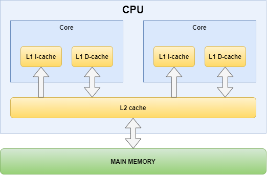
CPUs nowadays have more complex cache hierarchies, as they typically have per core L2 caches and an additional L3 cache shared across the cores (sometimes even an L4 cache too) in order to keep even more data closer to where it’s needed, but we chose the Core 2 Duo because its cache hierarchy captures the essence of multi-core processor cache organization. In particular, multi-core processors always feature at least two levels of caches:
- The closest level cache is private to the processor core
- The last level cache is shared across all processor cores
In addition, the first level consists of two caches, one dedicated for instruction caching and another dedicated for data caching, to acknowledge the usage pattern differences between code and data, as code is read-only from the perspective of the processor core and the instruction stream usually follows specific access patterns, while data is read/write and access pattern can be arbirary in the general case.
Unsurprisingly, modern GPUs use very similar cache hierarchies with one key difference: they have way more cores. This seemingly small difference, however, has all sorts of implications.
Cache Coherency
The fact that caches keep local copies of data that have their cannonical versions in memory introduces the problem of data non-coherence. As an example, if one core is modifying data stored in the core’s private data cache, then other cores may not see that update because they view the same memory location through their own caches. Also, if a device modifies data in the memory then that update may not be immediately visible to any of the processor cores, as they may be reading stale data from one of the caches in the hierarchy.
CPUs solve this problem by having cache coherency protocols in place between the different caches and the memory bus that use bus snooping or other solutions to detect updates to data and synchronize/invalidate cached data accordingly (e.g. see MOESI and MESIF protocols). This makes perfect sense for CPUs that only have a relatively small number of processing cores and it’s sort of a must have to support efficient data sharing between software running on arbitrary CPU cores/threads, due to the flexibility of the programming model that typically works under the assumption of a coherent memory system.
In case of GPUs the number of cores (compute units/streaming multiprocessors) is much larger and as such implementing cache coherency protocols would be too expensive both die area-wise and performance-wise. As a result, GPU caches are usually non-coherent, and require explicit flushing and/or invalidation of the caches in order to recohere (i.e. to have a coherent view of the data between the GPU cores and/or other devices). This, however, in practice doesn’t prove to be a problem due to the special programming model of GPUs where there is little to no way/need to do high-frequency data sharing between shaders/kernels running on different GPU cores. Specifically:
- shader invocations within individual draw or compute dispatch commands that run on different GPU cores may see non-coherent views of the same memory data, unless using coherent resources (see later), or issuing memory barriers within the shader that flush/invalidate the per core caches
- subsequent draw or compute dispatch commands may see non-coherent views of the same memory data, unless appropriate memory barriers are issued through the API that flush/invalidate the appropriate caches
- GPU commands and operations performed by other devices (e.g. CPU reads/writes) may see non-coherent views of the same memory data, unless appropriate synchronization primitives (e.g. fences or semaphores) are used to synchronize them, which implicitly insert the necessary memory barriers
This, of course, is not a set of formal rules but rather just a rough summary of what to expect, and individual GPU programming APIs may have different rules, default behaviors, and synchronization tools.
Per Core Instruction Cache
We will start exploring the per core caches of GPUs with the shader instruction cache, as that’s the simpler one.
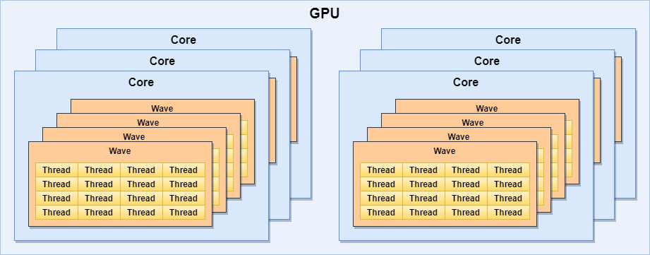
While the programming model and thus the hardware implementation of GPUs are very different to that of CPUs, the core building blocks and techniques used by them aren’t that dissimilar. As an example, prevalent GPU architectures use SIMD processing units, but instead of using them to enable vector instructions from individual threads, they use a SIMT (Single Instruction Multiple Thread) execution model where each lane is practically running a separate thread (shader invocation). This is a great model for GPUs as they typically run relatively simple programs over a large set of work items thus they benefit from being able to schedule instructions for a group of threads together instead of having to schedule them individually. Group of threads that are co-executed in this SIMT fashion (often in lock-step) form a wave (wavefront in AMD terminology, warp in NVIDIA terminology, subgroup in Vulkan terminology).
In addition, similar to the simultaneous multithreading (SMT) features of CPUs (e.g. hyper-threading), GPUs can also have multiple waves running on a single core. This enables increasing the number of independent instructions in the pipeline, but more importantly allow the GPU to execute instructions of other waves while a wave is waiting for data from memory/caches/etc. In practice a single GPU core can have thousands of threads running on it, albeit most only in turns. E.g.:
- An AMD GCN compute unit (CU) can have 40 waves in progress, 64 threads each, totalling up to 2560 threads / CU
- An NVIDIA Volta streaming multiprocessor (SM) can have 64 waves in progress, 32 threads each, totalling up to 2048 threads / SM
The effective number of threads that may run on any given GPU core may be much lower in practice than that due to various factors, but discussing the details of that is outside of the scope of this article.
What’s important to note, however, is that despite the huge number of threads running on a single GPU core, they usually all run the same code. For threads of a single wave this is true by definition due to the SIMT execution model. In fact, It’s quite common for the same code to be executed across waves from multiple GPU cores, as the number of work items a program is executed on in a typical GPU workload is even larger than what can fit on a single GPU core (e.g. a full-screen pass over a full HD image results in over 2 million thread invocations).
This means that a small per core instruction cache is more than satisfactory, even considering the enormous number of threads running on a single GPU core. Some GPUs go even further and share the instruction cache across multiple GPU cores (e.g. AMD’s GCN architecture shares a single 32KB instruction cache across a cluster of up to 4 compute units).
One thing to keep in mind from performance point of view is that on GPUs an instruction cache miss can potentially stall thousands of threads instead of just one, as in the case of CPUs, so generally it’s highly recommended for shader/kernel code to be small enough to completely fit into this cache.
Per Core Data Cache
Each GPU core usually has one or more dedicated shader data caches. In earlier GPU designs shaders could only read data from memory but not write to it, as typically shaders only needed to access texture and buffer inputs to perform their tasks, so per core data caches have been traditionally read-only. However, later architectures tailored for flexible GPGPU compute operations needed to support scattered writes to memory hence the need for a read/write data cache appeared. These caches typically use a write-through policy, i.e. writes are immediately propagated to the next cache level.
The typical size of the data cache of a GPU core is between 16KB and 128KB which is comparable to the usual 32KB L1 data cache size used by most CPUs. However, we cannot forget that this data cache services a significantly higher number of threads than in case of CPUs, and even though all threads on the GPU core usually run the same code, and threads within a single wave even run the same instruction at any given time, they still usually need to read different addresses each. That makes the capacity of the per code data cache of GPUs fall short by a long shot compared to their CPU equivalents, as illustrated in the table below:
| Processor Core | Data cache size | Max threads | Capacity / thread (4 waves) | Capacity / thread (max waves) |
|---|---|---|---|---|
| AMD GCN CU | 16 KB | 2560 (40x 64-wide waves) | 64 bytes | 6.4 bytes |
| AMD RDNA DCU | 2x 16 KB | 2560 (80x 32-wide waves) | 256 bytes | 12.8 bytes |
| NVIDIA Pascal SM | 24 KB | 2048 (64x 32-wide waves) | 192 bytes | 12 bytes |
| NVIDIA Volta SM (config A) | 32 KB | 2048 (64x 32-wide waves) | 256 bytes | 16 bytes |
| NVIDIA Volta SM (config B) | 64 KB | 2048 (64x 32-wide waves) | 512 bytes | 32 bytes |
| NVIDIA Volta SM (config C) | 96 KB | 2048 (64x 32-wide waves) | 768 bytes | 48 bytes |
NOTE: NVIDIA Volta L1 data cache can operate with different capacities (see later).
As it can be seen, the per core data cache size of GPUs is often quite small to be useful for traditional caching at high wave occupancy, i.e. to increase the performance of repeated accesses to the same memory location simply due to the sheer number of threads that may execute on a single GPU core, as they will inevitably evict each other’s data from the cache. This means that the per core data cache usually acts more as a coalescing buffer for memory operations rather than as a typical cache. E.g. a 32-wide wave executing on an RDNA core with each thread accessing an element from an array with 4-byte elements, one per work-item, will result in a single 128 byte cache line fetch, assuming that the array’s base address is appropriately aligned.
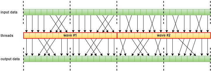
There is an important class of access patterns, however, where the true benefit of caching shows: if there is overlap between the memory locations accessed by threads of the same wave, or other waves on the same GPU core. While such access patterns are not uncommon in the general case either, it’s actually almost always the case when performing filtered texture lookups, as the 2×2 texel footprint fetched to produce a bilinearly filtered texture sample in e.g. a fragment shader thread will have overlaps with the texels needed by up to 8 “neighboring” fragment shader threads. Thus in these cases the average cache hit rate can be around or sometimes even beyond 75%.

NOTE: The 2×2 bilinear texel footprints sampled by neighboring fragments overlap with each other.
Thus reuse of cached data on GPUs usually does not happen in the time domain as in case of CPUs (i.e. subsequent instructions of the same thread accessing the same data multiple times), but rather in the spatial domain (i.e. instructions of different threads on the same core accessing the same data). Accordingly, using memory as temporary storage and relying on caching for fast repeated access is not a good idea on GPUs, unlike on CPUs. However, the larger register space and the availability of shared memory make up for that in practice.
The extreme case of data reuse across threads is when all threads of one or more waves need to read data from the same address. This is quite common, as shaders/kernels often access constant data or other low-frequency data (e.g. workgroup-specific data in compute shaders). In order to increase the performance of such accesses, many GPUs have dedicated uniform data caches (sometimes called scalar or constant cache). The benefit of having a separate cache for this purpose is that it ensures that such low-frequency data doesn’t get evicted from the data cache by high-frequency data accesses that would otherwise happen if they’d be stored in the same cache under a common replacement policy.
Similar to code, such uniform data is often shared not just across waves within a single GPU core but across waves of multiple GPU cores, so this is another cache that is a good candidate for being shared across multiple GPU cores (e.g. AMD’s GCN architecture shares a single 16KB scalar cache across a cluster of up to 4 compute units).
Device Wide Cache
The per core and other lower level caches of GPUs are served by a device wide cache that provides coherent cached data across the cores, and it’s typically the last cache level in the hierarchy with a few notable exceptions. This is a read/write cache that usually also supports atomic operations. In fact, all atomic operations on memory backed data performed by the shaders/kernels are handled here, skipping the lower level caches in the process. Thus atomic operations by definition are coherent across threads running on different GPU cores, although, that does not guarantee that regular reads will see the results of atomics, as those will continue to be served by default from the per core data caches.
In order to support coherent access to mutable data shared across multiple cores, GPUs usually have special instructions or instruction variants to bypass the non-coherent per core caches even for regular non-atomic read or write operations. Although not all GPU programming APIs expose such fine grained control, there is always some mechanism to enable such coherent access to a resource. As an example, GLSL uses the “coherent” qualifier to mark an entire resource to be always accessed through memory operations that bypass the caches that are non-coherent across the GPU cores.
This feature comes handy not just when the shader invocations within a single draw or compute dispatch command need to coherently share mutable data, but also for data sharing between subsequent commands, as by using device wide coherent memory operations we can avoid having to flush/invalidate the per core caches between the commands which eliminates some or all of the synchronization related stall/bubble between the dependent operations.
Naturally, using coherent memory operations may be detrimental to performance as we discard the benefits of the lower level caches, however, for typical per-thread data accesses, let those be input data reads or output data writes, where requests across a wave coalesce into entire cache line sized data transactions, there should be no additional overhead. This is actually quite common in case of image processing shaders/kernels where each wave processes a corresponding 2D tile of an image, or other transformations where the threads of each wave read or write a contiguous, aligned range of the input or output data (typically arranged in a structure-of-arrays layout).
NOTE: the thread-to-data mapping does not necessarily have to be one-to-one (e.g. array[threadID]).
This optimization technique usually provides benefits if there is sufficient non-dependent work that can be scheduled for execution between the “producer” and “consumer” workloads that perform data sharing through coherent writes and reads, respectively, as it allows using a completion-only dependency between the two, without cache control operations such as the flushing/invalidation of the per core caches (e.g. a Vulkan event wait operation without a memory barrier).
It’s also worth noting that some architectures have additional caches between the device wide cache and the per core caches (e.g. the new L1 cache present on AMD’s RDNA architecture), however, that shouldn’t affect the validity of this technique in general.
But back to the device wide cache, when looking at its size, it’s still relatively small, as even if we compare the typical sizes on high-end GPUs, their 4MB-6MB size falls quite short compared to the L3 cache size of CPUs which serves a similar purpose, with the notable exception of AMD’s new “Big Navi” which features an additional level of device wide cache with a gigantic 128MB capacity, but that is more about compensating for its relatively narrow memory bus rather than filling the traditional role of the device wide cache of GPUs.
| GPU | Device wide cache size | Max threads | Capacity / thread (4 waves / core) | Capacity / thread (max waves) |
|---|---|---|---|---|
| AMD Polaris 20 (GCN) | 2 MB | 92160 (2560 x 36 CU) | 227.5 bytes | 22.75 bytes |
| AMD Navi 10 (RDNA) | 4 MB | 102400 (2560 x 40 CU) | 819.2 bytes | 40.96 bytes |
| NVIDIA GP100 (Pascal) | 4 MB | 122880 (2048 x 60 SM) | 546.13 bytes | 34.13 bytes |
| NVIDIA GV100 (Volta) | 6 MB | 163840 (2048 x 80 SM) | 614.4 bytes | 38.4 bytes |
As it can be seen, these cache capacities per thread are more likely to be useful for traditional caching, though it still shows that GPUs are primarily designed to process a huge number of relatively small data elements compared to CPUs which usually operate on significantly larger data sets using a smaller number of threads.
On a note about APUs and SoCs, the GPUs found on such hardware usually don’t have a dedicated device wide cache, instead they share the last level cache with the CPU.
Shared Memory
On modern GPUs each core has its own shared memory that is primarily used to share data between compute threads (or compute shader invocations) belonging to the same workgroup, and even supports atomic operations. Shared memory is not cache, but a type of scratchpad memory, but we mention it here nonetheless because it serves a similar purpose to that of caches in the sense that it enables keeping repeatedly used data close to the processing units.
The difference between caches and scratchpad memory is that while caches automatically manage the set of data they currently store, scratchpad memory is managed by the application software thus shader/kernel code can explicitly transfer data between memory and the scratchpad.
Another reason we mention shared memory, because NVIDIA went with the interesting idea of combining their L1 data cache and shared memory into a single component. This approach first appeared on their Kepler architecture, though that architecture still had a separate read-only texture cache. Maxwell and Pascal unified the L1 data cache and the texture cache, but they had a separate shared memory partition (similar to AMD’s solution). Finally, since their Volta architecture the unified data cache and shared memory are all part of a single component.
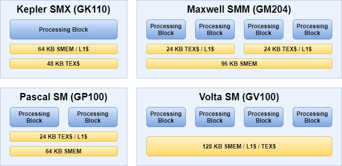
SMEM: shared memory
L1$: L1 read-write data cache
TEX$: read-only texture cache
This solution enables NVIDIA to dynamically partition this combined data storage component into various sizes reserved for data cache and shared memory usage. On the Ampere architecture it’s possible to use the entire 128 KB (or 192 KB) as per core data cache in case no shared memory is needed, which may be the case for graphics-only workloads. In addition, this likely also enables NVIDIA to directly load data from the L2 cache into shared memory, considering that it’s served by the same component as the L1 data cache, however, it’s impossible to verify that as NVIDIA’s ISA (instruction set architecture) is not public.
There are noteworty ideas related to shared memory on AMD GPUs too. In particular, besides the per core shared memory, the LDS (local data share), AMD GCN and RDNA GPUs also have a device wide shared memory called the GDS (global data share), which works similarly, but allows for sharing data across all threads running on any of the GPU cores, including fast, global, unordered atomic operations. Unfortunately, to date, no GPU programming API exposes access to GDS directly.
Other caches
So far, we only talked about caches used to accelerate memory accesses performed by the shader cores, but GPUs usually employ other caches that serve the various fixed function hardware components that implement certain stages or functions of the graphics pipeline. An example of such a cache is the vertex attribute cache that was traditionally used to cache vertex attribute values before dispatching the corresponding vertex shader invocations. Nowadays, due to the increased programmability of the geometry processing stages, there is usually no need for such a dedicated cache as attribute data reads often happen from within the shaders, either explicitly or implicitly, especially in case of modern geometry pipelines using tessellation, geometry shaders, or mesh shaders.
At the other end of the graphics pipeline we usually have another set of caches, typically referred to as the ROP (raster operation) or RB (render backend) caches, that provide caching for framebuffer attachment (render target) operations. These still exist on modern immediate mode renderer (IMR) GPUs (not to be confused with the immediate mode of the OpenGL API), because framebuffer operations have specific enough access patterns, due to the way how rasterization works, to justify a tailored solution that provides the best performance for the specific usage. Also, framebuffer memory accesses on IMR GPUs generally happen separately from fragment shader execution, being issued by dedicated ROP units that provide a few other functionalities (e.g. blending and ensuring that framebuffer updates happen according to the incoming primitive order).
There are usually multiple ROP caches across a GPU, each serving one or more ROP units, and generally each ROP cache consists of a separate depth/stencil and color cache, again due to the specific needs of depth/stencil attachments versus color attachments. These caches are, once again, typically non-coherent with respect to its siblings, including the per-core shader caches, and they may or may not be backed by the same device wide cache(s) as the per-core caches.
Until the dawn of compute shaders, the most common GPU cache synchronization operation was to sync writes done through the ROP caches with reads done through the per-core shader caches (render-to-texture then read results, e.g. shadow mapping, reflection maps). Such data dependencies are still common, even though compute shaders are more often used for image-space processing nowadays (e.g. post-processing, deferred shading/lighting), so it’s best to keep the ROP caches as close as possible to the per-core shader caches in the cache hierarchy. It thus comes at no surprise that GPUs which traditionally didn’t back their ROP caches with the device wide cache moved to a design where they are.

Tile-based renderer (TBR) GPUs, prevalent on mobile SoCs, work in a different fashion thus they don’t have ROP caches as IMR GPUs. These GPUs split the framebuffer space into a grid of tiles and perform rasterization and fragment/pixel processing for each tile separately. This approach enables them to minimize the amount of external memory accesses the GPU needs to perform during fragment/pixel processing by loading framebuffer data corresponding to each tile before processing the tile and then storing the results back to memory afterwards. The storage where the currently processed tile’s framebuffer data resides is usually referred to as on-chip/local tile memory.
Tile memory generally functions as a scratchpad memory, similar to shared memory, in fact it’s likely that actual implementations use the same physical storage for both. It’s a scratchpad memory because the data it holds is explicitly controlled by the application, although not always directly. In particular, the Vulkan graphics API provides dedicated functionalities to control when, how, and what data is loaded to the tile memory from video memory or stored from tile memory to video memory. The application controls the behavior through the per-attachment load/store operations and other parameters of Vulkan render pass objects.
Finally, it’s also worth noting that modern GPUs use virtual memory addressing thus they also use a separate cache hierarchy of translation lookaside buffers (TLBs) to accelerate virtual to physical address translation. On integrated solutions the TLB hierarchy may be shared with with the CPU, while in case of discrete GPUs there’s always a dedicated TLB hierarchy on the chip.
Conclusion
We managed to cover the key aspects of the cache hierarchy of GPUs, how they compare to the cache hierarchy of CPUs, and what are the main design and implementation disparities between the two. We’ve also seen how these differences affect the programming model, in particular, that the non-coherent caches of the GPU require special attention from the application programmer when it comes to data synchronization across work items, and across subsequent draw and compute dispatch commands.
GPUs and CPUs are built for different types of tasks. CPUs run only a few threads in parallel but each have large and complex code and data sets they operate on, while GPUs execute orders of magnitudes larger number of threads simultaneously yet typically most share the same code and access relatively small amount of data per thread. Due to this, despite the similarities of the actual cache hierarchies used by the two processor types, the actual usage pattern of the caches is significantly different in practice. Keeping that in mind is paramount to achieve good performance and is often the reason behind why naive ports of CPU-centric algorithms perform poorly on GPUs.
Beyond caches, we also talked about different types of scratchpad memories available on today’s GPUs, and how they complement caches in order to further improve data access performance.
All the information presented in this article related to specific GPU cache types, hierarchies, and sizes was aggregated based on the architecture whitepapers and other publicly available materials released by the hardware vendors of the corresponding GPU or GPU generation. For further reading, please check out the list below:
- AMD GCN Architecture Whitepaper
- AMD GCN Gen1 Instruction Set Architecture
- AMD GCN Gen2 Instruction Set Architecture
- AMD GCN Gen3 Instruction Set Architecture
- AMD Vega Instruction Set Architecture
- AMD RDNA Architecture Whitepaper
- AMD RDNA 1 Instruction Set Architecture
- AMD RDNA 2 Instruction Set Architecture
- NVIDIA Kepler Architecture Whitepaper
- NVIDIA Maxwell Architecture Whitepaper
- NVIDIA Pascal Architecture Whitepaper
- NVIDIA Volta Architecture Whitepaper
- NVIDIA Turing Architecture Whitepaper
- NVIDIA Ampere Architecture Whitepaper